| CPC H02M 3/155 (2013.01) | 14 Claims |
|
1. A control circuit for a power converter, the power converter comprising a switching circuit, wherein: the switching circuit comprises a first switching transistor and a second switching transistor; and the switching circuit is configured to receive an input voltage and responsively convert the input voltage into an output voltage, wherein a constant on-time control is performed by the control circuit for the power converter, and wherein the control circuit comprises:
a comparator provided with a first input, a second input and an output, wherein: the first input of the comparator is configured to receive at least a reference signal; the second input of the comparator is configured to receive at least a feedback signal; and the output of the comparator is configured to output a comparison signal, and wherein the feedback signal is derived from the output voltage;
an on-time generation circuit configured to generate an on-time signal, wherein a first control signal for controlling the first switching transistor and a second control signal for controlling the second switching transistor are derived from the on-time signal by a drive circuit;
a ramp compensation circuit configured to generate a ramp compensation signal, wherein the first or second input of the comparator receives a superposition of the ramp compensation signal and the feedback signal, wherein the ramp compensation signal has a first slope peak in a steady state and has a second slope peak lower than the first slope peak during a transient response to a load current jump, and wherein a transition from the first slope peak to the second slope peak is irrespective of DC bias settings of the ramp compensation circuit,
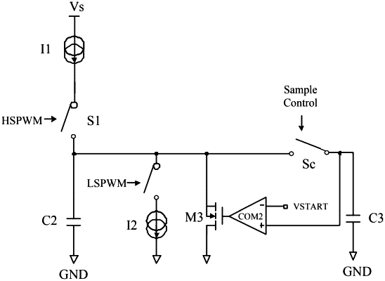
wherein the ramp compensation circuit comprises an initial value resetting circuit, and wherein the initial value resetting circuit comprises:
a first power transistor provided with a first source, a first drain and a first gate, wherein: the first source is connected to a second terminal of a first switch; and the first drain is connected to the reference ground or a supply voltage;
a second comparator provided with a first input, a second input and an output, wherein: the first input of the second comparator receives an initial value for each period of the ramp compensation signal; and the output of the second comparator is connected to the first gate;
a sampling control switch provided with a first terminal, a second terminal and a control terminal, wherein: the first terminal of the sampling control switch is connected to the first source of the first power transistor; the second terminal of the sampling control switch is connected to the second input of the second comparator; and the control terminal of the sampling control switch receives a sampling control signal for closing the sampling control switch at the end of each operational period; and
a holding capacitor provided with a first terminal and a second terminal, wherein: the first terminal of the holding capacitor is connected to the second terminal of the sampling control switch; and the second terminal of the holding capacitor is connected to the reference ground.
|