| CPC H02H 7/18 (2013.01) [H02H 1/0007 (2013.01); H02J 7/0013 (2013.01); H02J 7/345 (2013.01); H02J 9/061 (2013.01)] | 17 Claims |
|
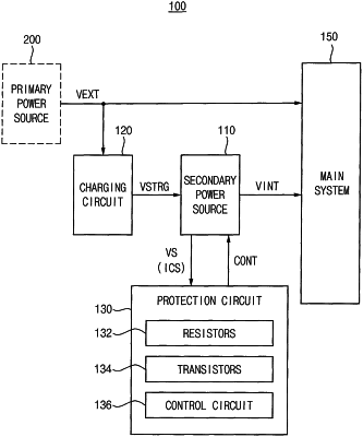
1. A storage device comprising:
a secondary power source including a plurality of capacitors, the secondary power source configured to be charged based on a charging voltage, and configured to generate an internal power supply voltage;
a charging circuit configured to generate the charging voltage based on an external power supply voltage;
a protection circuit configured to detect whether at least one of the plurality of capacitors is defective, and configured to deactivate at least one defective capacitor among the plurality of capacitors based on the at least one of the plurality of capacitors being detected as defective; and
a main system configured to operate based on the external power supply voltage or the internal power supply voltage, and
wherein the protection circuit includes:
a plurality of resistors connected to first ends of the plurality of capacitors;
a plurality of transistors connected to second ends of the plurality of capacitors; and
a control circuit configured to detect whether the at least one of the plurality of capacitors is defective based on a first current among a plurality of currents associated with the plurality of capacitors, the first current being associated with the at least one of the plurality of capacitors, and
configured to deactivate the at least one defective capacitor by outputting a control signal to at least one of the plurality of transistors associated with the at least one of the plurality of capacitors,
wherein:
a number of the plurality of capacitors, a number of the plurality of resistors, and a number of the plurality of transistors are equal to one another,
each one of the plurality of resistors and each one of the plurality of transistors are respectively connected to each one of the plurality of capacitors,
the plurality of capacitors include a first capacitor,
the plurality of resistors include a first resistor connected between the charging voltage and a first end of the first capacitor,
the plurality of transistors include a first transistor connected between a second end of the first capacitor and a ground voltage,
the control signal includes a first control signal applied to the first transistor, and
the control circuit is configured to:
sense a first voltage at the first end of the first capacitor using the first resistor,
calculate the first current based on the charging voltage and the first voltage, and
determine, based on the first current, whether the first capacitor is defective,
wherein based on a determination that the first capacitor is normal, the control circuit is configured to:
generate a charging voltage control signal to compensate for a voltage drop by the first resistor and the first transistor, and
output the charging voltage control signal to the charging circuit.
|