| CPC H01S 5/18338 (2013.01) [H01S 5/0425 (2013.01)] | 15 Claims |
|
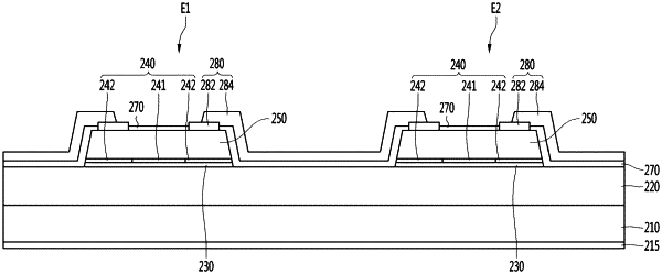
1. A surface-emitting laser device comprising:
a first reflective layer;
an active region disposed on the first reflective layer;
a plurality of aperture regions disposed on the active region and including an aperture and an insulating region;
a second reflective layer disposed on the aperture region; and
a first electrode and a second electrode electrically connected to the first reflective layer and the second reflective layer, respectively,
wherein an outer periphery of each insulating region of the plurality of aperture regions is circular,
wherein an outer periphery of the aperture comprises a polygonal shape,
wherein a size of the aperture is greater than the shortest distance from a polygonal edge of the aperture to an outer edge of the insulating region, and
wherein a distance between centers of each of the closest apertures in the plurality of aperture regions is greater than twice a radius of each aperture region and less than 3 times, and a size of the aperture region is a sum of half size of the aperture and a shortest distance from the polygonal edge to the outside of the insulating region.
|