| CPC H01Q 1/1271 (2013.01) [H01Q 9/0414 (2013.01)] | 14 Claims |
|
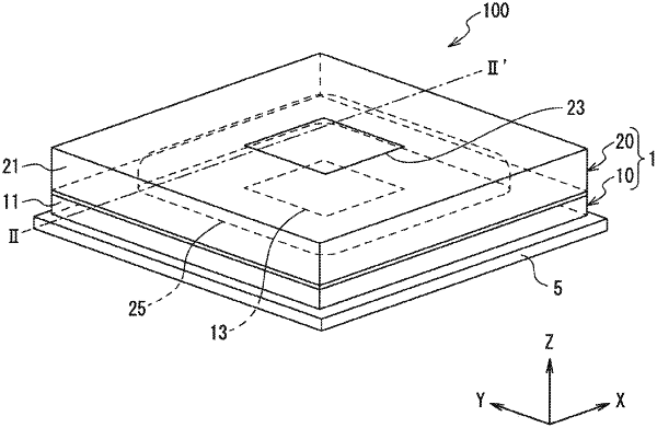
1. An antenna device, comprising:
a first antenna element; and
a second antenna element on a face side of the first antenna element, wherein
the first antenna element includes
a first glass substrate, and
a first patch antenna on the first glass substrate,
the second antenna element includes
a second glass substrate, and
a second patch antenna on the second glass substrate,
the second glass substrate includes, as an air gap, a second recessed portion open to a face side of the second glass substrate facing the first glass substrate,
the second patch antenna is on a side opposite to a bottom face of the second recessed portion, and
at least a part of the first patch antenna faces the second patch antenna with the air gap interposed therebetween.
|