| CPC H01L 33/62 (2013.01) [H01L 25/0753 (2013.01)] | 6 Claims |
|
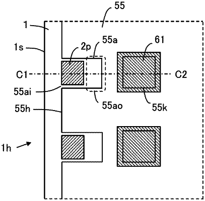
1. A wiring board comprising:
a substrate comprising a first surface, a second surface which is opposite to the first surface, and a side surface;
an electrode located at a portion of a side of the first surface;
an insulating layer disposed on the substrate; and
a side wiring disposed so as to extend from the electrode via the side surface to the second surface,
an end of the insulating layer with a cutaway portion extending in an inward direction of the insulating layer,
the electrode being disposed in an entrance-side part of the cutaway portion, and the cutaway portion comprising a bottom-side part constituting an inward area which is free of the electrode,
the electrode being entirely received in the cutaway portion.
|