| CPC H01L 33/62 (2013.01) [H05K 1/028 (2013.01); H05K 3/06 (2013.01); H01L 2933/0066 (2013.01)] | 16 Claims |
|
1. A method for manufacturing a side wire for a substrate, comprising:
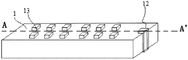
forming a plurality of first pattern structures on a side surface of the substrate, wherein a gap between any adjacent two of the plurality of first pattern structures connects a top surface and a bottom surface of the substrate to each other;
forming a conductive material film covering the side surface of the substrate; and
removing the plurality of first pattern structures and a portion of the conductive material film attached on the plurality of first pattern structures, and maintaining a portion of the conductive material film located between any adjacent two of the plurality of first pattern structures as the side wire,
wherein the forming a plurality of first pattern structures on a side surface of the substrate comprises:
forming a plurality of first pattern preliminary structures on the side surface of the substrate by using a predetermined ink, wherein a gap between any adjacent two of the plurality of first pattern preliminary structures connects the top surface and the bottom surface of the substrate to each other, and the predetermined ink comprises a first solvent and a self-assembly material; and
removing the first solvent in the predetermined ink to cause the self-assembly material to combine into a unitary structure so as to obtain the plurality of first pattern structures.
|