US 11,984,545 B2
Method of manufacturing a light emitting device
Naoyuki Urasaki, Chikusei (JP); and Kanako Yuasa, Saitama (JP)
Assigned to SHENZHEN JUFEI OPTOELECTRONICS CO., LTD., Shenzhen (CN)
Filed by Shenzhen Jufei Optoelectronics Co., Ltd., Shenzhen (CN)
Filed on Dec. 29, 2021, as Appl. No. 17/565,020.
Application 16/392,900 is a division of application No. 15/865,299, filed on Jan. 9, 2018, granted, now 10,326,063, issued on Jun. 18, 2019.
Application 15/865,299 is a division of application No. 15/603,618, filed on May 24, 2017, granted, now 10,205,072, issued on Feb. 12, 2019.
Application 15/603,618 is a division of application No. 12/303,188, granted, now 9,673,362, issued on Jun. 6, 2017, previously published as PCT/JP2007/060385, filed on May 21, 2007.
Application 17/565,020 is a continuation of application No. 17/169,054, filed on Feb. 5, 2021.
Application 17/169,054 is a continuation of application No. 16/392,900, filed on Apr. 24, 2019, granted, now 10,950,767, issued on Mar. 16, 2021.
Claims priority of application No. 2006-154652 (JP), filed on Jun. 2, 2006.
Prior Publication US 2022/0123187 A1, Apr. 21, 2022
Int. Cl. H01L 33/00 (2010.01); H01L 33/38 (2010.01); H01L 33/48 (2010.01); H01L 33/50 (2010.01); H01L 33/52 (2010.01); H01L 33/60 (2010.01); H01L 23/00 (2006.01); H01L 33/62 (2010.01)
CPC H01L 33/60 (2013.01) [H01L 33/38 (2013.01); H01L 33/486 (2013.01); H01L 33/50 (2013.01); H01L 33/52 (2013.01); H01L 24/45 (2013.01); H01L 24/73 (2013.01); H01L 33/62 (2013.01); H01L 2224/16245 (2013.01); H01L 2224/32245 (2013.01); H01L 2224/45144 (2013.01); H01L 2224/48091 (2013.01); H01L 2224/48247 (2013.01); H01L 2224/48465 (2013.01); H01L 2224/73265 (2013.01); H01L 2924/181 (2013.01); H01L 2924/1815 (2013.01)] 5 Claims
OG exemplary drawing
 
1. A method of manufacturing a light emitting device, comprising:
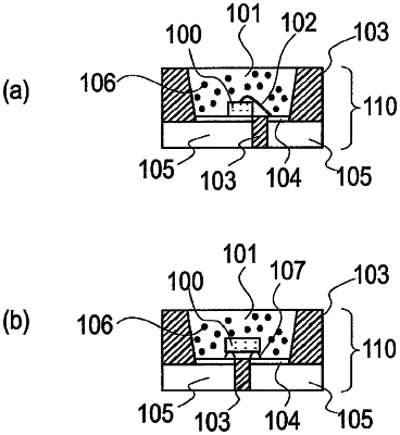
disposing at least one light emitting element on a recessed part of a resin package, wherein the resin package having the recessed part comprises:
a resin molding, wherein a composition of the resin molding includes a white pigment having a particle size from 0.1 μm to 50 μm; and
at least one lead electrode with a metal film plated on a main face, wherein the resin molding is disposed on a portion of the main face of the at least one lead electrode and is not in contact with a rear face of the at least one lead electrode,
wherein an outer surface of the resin molding and an outer surface of the at least one lead electrode are coplanar at an outer surface of the resin package;
wherein the at least one light emitting element is disposed on the main face of the at least one lead electrode.