US 11,984,539 B2
Light-emitting element, manufacturing method therefor, and display device having light-emitting element
Su Mi Moon, Yongin-si (KR); Eun Ju Kim, Yongin-si (KR); and Hyun Min Cho, Yongin-si (KR)
Assigned to SAMSUNG DISPLAY CO., LTD., Yongin-si (KR)
Appl. No. 17/297,870
Filed by SAMSUNG DISPLAY CO., LTD., Yongin-si (KR)
PCT Filed Jun. 20, 2019, PCT No. PCT/KR2019/007465
§ 371(c)(1), (2) Date May 27, 2021,
PCT Pub. No. WO2020/111425, PCT Pub. Date Jun. 4, 2020.
Claims priority of application No. 10-2018-0148788 (KR), filed on Nov. 27, 2018.
Prior Publication US 2022/0037562 A1, Feb. 3, 2022
Int. Cl. H01L 33/44 (2010.01); H01L 25/16 (2023.01); H01L 33/00 (2010.01); H01L 33/24 (2010.01)
CPC H01L 33/44 (2013.01) [H01L 25/167 (2013.01); H01L 33/0062 (2013.01); H01L 33/0066 (2013.01); H01L 33/24 (2013.01); H01L 2933/0025 (2013.01)] 19 Claims
OG exemplary drawing
 
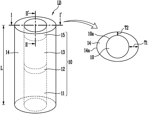
1. A light emitting element comprising:
an emission stacked pattern having a rod shape, the emission stacked pattern including:
a first conductive semiconductor layer;
an active layer disposed on the first conductive semiconductor layer; and
a second conductive semiconductor layer disposed on the active layer; and
an insulating film surrounding an outer surface of the emission stacked pattern and having a non-uniform thickness.