| CPC H01L 33/387 (2013.01) [H01L 33/405 (2013.01); H01L 33/42 (2013.01); H01L 33/502 (2013.01); H01L 33/62 (2013.01)] | 14 Claims |
|
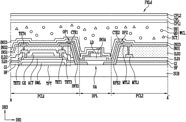
1. A display device comprising:
a substrate;
a first circuit part and a second circuit part on the substrate and spaced from each other in a first direction;
an emission part between the first circuit part and the second circuit part, the emission part being located between the first circuit part and the second circuit part in a direction parallel to the substrate; and
a first insulation layer between the substrate and the emission part,
wherein the first circuit part comprises a first electrode extending to the emission part, and a third electrode on the first electrode,
wherein the second circuit part comprises a second electrode extending to the emission part, and a fourth electrode on the second electrode,
wherein the emission part comprises a light emitting element located between the first electrode and the second electrode, at least a portion of the third electrode being in contact with a first end of the light emitting element and at least a portion of the fourth electrode being in contact with a second end of the light emitting element,
wherein the first insulating layer continuously covers the first and second electrodes from a location below the light emitting element to a portion of the first and second electrodes farthest away from the substrate, respectively,
wherein the display device further comprises a wavelength conversion layer on the light emitting element,
wherein the wavelength conversion layer comprises a wavelength conversion particle and a scattering particle, and
wherein the wavelength conversion particle comprises a quantum dot.
|