| CPC H01L 33/382 (2013.01) [H01L 33/46 (2013.01); H01L 33/62 (2013.01); H01L 33/32 (2013.01); H01L 33/42 (2013.01)] | 20 Claims |

|
1. A semiconductor light emitting device, comprising:
a first electrode layer having a first region and a second region;
a light emitting structure on the first region of the first electrode layer, the light emitting structure including:
a first conductivity-type semiconductor layer,
an active layer,
a second conductivity-type semiconductor layer, and
holes connected to the first conductivity-type semiconductor layer through the active layer;
a transparent electrode layer between the first region of the first electrode layer and the light emitting structure, the transparent electrode layer contacting the second conductivity-type semiconductor layer;
an interlayer insulating layer between the transparent electrode layer and the first electrode layer, the interlayer insulating layer including:
first openings respectively connected to the holes of the light emitting structure, and
second openings connected to the transparent electrode layer, each one of the first openings and at least one of the second openings, closest to the one of the first openings, defining one group, such that the first openings correspond to a plurality of groups, respectively;
a second electrode layer between the first electrode layer and the interlayer insulating layer, the second electrode layer being connected to the transparent electrode layer through the second openings, and the second electrode layer being separated from the first electrode layer and extending onto the second region of the first electrode layer;
an electrode pad on the second electrode layer to overlap the second region; and
contact electrodes through the second electrode layer, the interlayer insulating layer, and the transparent electrode layer, the contact electrodes being connected to the first conductivity-type semiconductor layer through the holes,
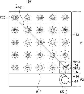
wherein the plurality of groups includes at least a first group and a second group, the first group being closer to the electrode pad than the second group is, and a first distance between the one of the first openings and the at least one of the second openings in the first group being greater than a second distance between the one of the first openings and the at least one of the second openings in the second group.
|