| CPC H01L 33/32 (2013.01) [H01L 33/0075 (2013.01); H01L 33/12 (2013.01); H01L 33/58 (2013.01); H01S 5/026 (2013.01); H01S 5/34333 (2013.01)] | 10 Claims |
|
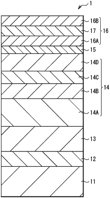
1. A light emitting device comprising:
a first layer including Alx2Inx1Ga(1-x1-x2) N (0<x1<1, 0≤x2<1);
a second layer that is provided on the first layer and includes Aly2Iny1Ga(1-y1-y2) N (0<y1<1, 0≤y2<1); that is lattice relaxed with respect to the first layer; and
a third layer that is provided on the second layer, includes Alz2Inz1Ga(1-z1-z2) N (0<z1<1, 0≤z2<1) that is lattice relaxed with respect to the second layer, and includes an active layer, wherein
a lattice constant aGAN of GaN in an in-plane direction, a lattice constant a1 of the first layer in an in-plane direction, a lattice constant a2 of the second layer in an in-plane direction, and a lattice constant a3 of the third layer in an in-plane direction have a relationship of aGAN <a2<a1, a3.
|