| CPC H01L 33/22 (2013.01) [A61L 9/20 (2013.01); H01L 33/382 (2013.01); H01L 33/44 (2013.01); H01L 33/486 (2013.01); C02F 1/325 (2013.01); C02F 2201/3222 (2013.01); C02F 2303/04 (2013.01)] | 18 Claims |
|
1. A semiconductor device comprising:
a conductive substrate;
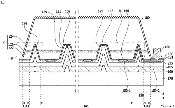
a semiconductor structure arranged on the conductive substrate, including a first conductive type semiconductor layer, a second conductive type semiconductor layer, and an active layer arranged between the first conductive type semiconductor layer and the second conductive type semiconductor layer, and including a plurality of recesses which pass through the second conductive type semiconductor layer and the active layer, and up to a partial region of the first conductive type semiconductor layer;
a first electrode configured to electrically connect the first conductive type semiconductor layer and the conductive substrate;
a second electrode electrically connected to the second conductive type semiconductor layer; and
an insulating layer arranged in the plurality of recesses,
wherein the plurality of recesses include a first recess extending along an outer surface of the semiconductor structure and a plurality of second recesses arranged at an inner side of the first recess,
wherein the first electrode includes a plurality of protruding electrodes extending to the inside of the plurality of second recesses so as to be electrically connected to the first conductive type semiconductor layer,
wherein the active layer includes an inactive area arranged between a side surface of the semiconductor structure and the first recess, and an active area arranged on the inner side of the first recess,
wherein an emission intensity of the inactive area is less than an emission intensity of the active area,
wherein the plurality of second recesses include a plurality of inner recesses in which a number of closest recesses is N and a plurality of outer recesses in which a number of closest recesses is less than N,
wherein the active area includes a second-first region arranged at an outer side based on a closed-loop connecting centers of closest outer recesses among the plurality of outer recesses, and a second-second region arranged at an inner side of the closed-loop, and
wherein a ratio of an emission intensity of the second-second region and an emission intensity of the second-first region is 1:0.5 to 1:0.8.
|