| CPC H01L 33/06 (2013.01) [H01L 29/00 (2013.01); H01L 33/10 (2013.01); H01L 33/025 (2013.01); H01L 33/145 (2013.01); H01L 33/32 (2013.01)] | 20 Claims |
|
1. A heterostructure comprising:
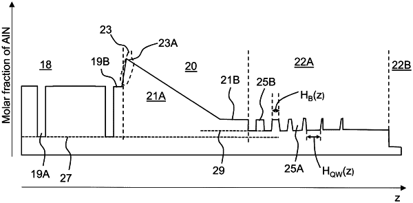
an active region including at least one quantum well and at least one barrier;
an electron blocking layer located adjacent to the active region, wherein the electron blocking layer includes a region of graded composition formed by a composition having an aluminum nitride molar fraction that continuously increases or continuously decreases with distance from the active region; and
a p-type superlattice layer located adjacent to the electron blocking layer, wherein the p-type superlattice layer includes at least one well and at least one barrier, wherein an aluminum nitride molar fraction of each of the at least one well and each of the at least one barrier in the p-type superlattice layer is lower than an average aluminum nitride molar fraction of the region of graded composition in the electron blocking layer;
a p-type contact layer located adjacent to the p-type superlattice layer.
|