| CPC H01L 31/107 (2013.01) [B60W 30/00 (2013.01); G01S 7/4861 (2013.01); G01S 17/10 (2013.01); H01L 27/1446 (2013.01); H01L 31/02005 (2013.01); H01L 31/02027 (2013.01); H01L 31/03529 (2013.01); B60W 2420/40 (2013.01)] | 27 Claims |
|
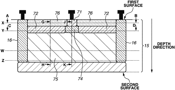
1. A photodetection apparatus comprising:
a semiconductor substrate having a first surface and a second surface opposite to the first surface; and
a pixel unit having a plurality of pixels each including an avalanche diode, the plurality of pixels being arranged on the semiconductor substrate,
wherein the avalanche diode includes:
an avalanche amplification region including a first semiconductor region of a first conductivity type and a part of a second semiconductor region of a second conductivity type, the first semiconductor region being arranged in a first depth and the second semiconductor region being arranged in a second depth greater than the first depth with respect to the first surface;
an electric charge generation region arranged in a third depth greater than the second depth with respect to the first surface; and
an isolation portion that isolates each of the plurality of pixels arranged in the pixel unit,
wherein an area of the avalanche amplification region is smaller than an area of the charge generation region in a plane view, and the area of the avalanche amplification region is smaller than an area of the second semiconductor region in a plane view.
|