| CPC H01L 31/02327 (2013.01) [H01L 31/102 (2013.01)] | 20 Claims |
|
11. A light sensing device, comprising:
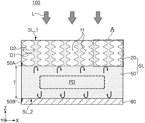
a semiconductor layer including a distributed Bragg reflector including a first surface of the semiconductor layer, and a photoelectric conversion unit including a second surface of the semiconductor layer, and the distributed Bragg reflector has a plurality of holes each having, in a cross-sectional view, a width gradually changing from a first width to a second width according to a width change period;
a first electrode in one region of the semiconductor layer; and
a second electrode on the second surface of the semiconductor layer and having a reflective metal,
wherein the width change period extends parallel to a direction extending from the first surface of the semiconductor layer to the second surface of the semiconductor layer.
|