| CPC H01L 31/02027 (2013.01) [G02B 3/06 (2013.01); H01L 27/14605 (2013.01); H01L 27/1461 (2013.01); H01L 27/14621 (2013.01); H01L 27/14623 (2013.01); H01L 27/14627 (2013.01); H01L 27/14629 (2013.01); H01L 27/1463 (2013.01); H01L 27/14636 (2013.01); H01L 27/14643 (2013.01); H01L 27/14645 (2013.01); H01L 27/14649 (2013.01); H01L 31/02327 (2013.01); H01L 31/055 (2013.01); H01L 31/107 (2013.01); H01L 27/1464 (2013.01); H04N 25/63 (2023.01)] | 20 Claims |
|
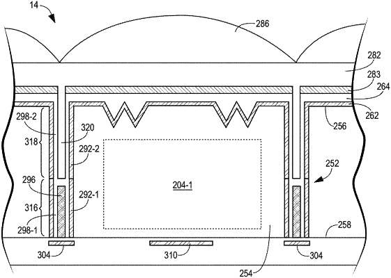
1. A semiconductor device comprising:
a substrate having first and second opposing surfaces;
a photosensitive element formed in the substrate;
a trench in the substrate that extends around the photosensitive element;
a metal filler in a first subset of the trench; and
a dielectric filler in a second, different subset of the trench, wherein the dielectric filler is interposed between the metal filler and the first surface and wherein the dielectric filler has a greater depth thickness between the metal filler and the first surface than a distance between the metal filler and the second surface.
|