| CPC H01L 29/7869 (2013.01) [H01L 29/24 (2013.01); H01L 29/4908 (2013.01); H01L 29/66742 (2013.01)] | 23 Claims |

|
1. A thin-film transistor, comprising:
a base substrate;
a semiconductor layer on the base substrate, the semiconductor layer comprising:
a first oxide semiconductor layer; and
a second oxide semiconductor layer on the first oxide semiconductor layer;
a gate electrode spaced apart from the semiconductor layer and partially overlapping the semiconductor layer;
a gate insulating layer between the semiconductor layer and the gate electrode; and
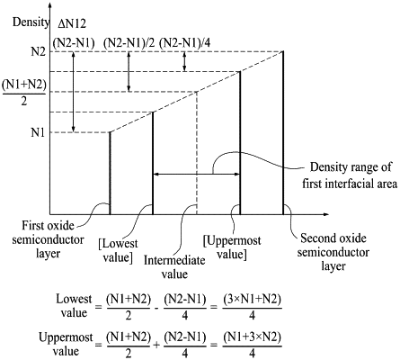
a first mixture area between the first oxide semiconductor layer and the second oxide semiconductor layer,
wherein a concentration of gallium (Ga) in the second oxide semiconductor layer is higher than a concentration of gallium (Ga) in the first oxide semiconductor layer,
wherein the gate insulating layer comprises silicon and oxygen,
wherein the gate insulating layer comprises hydrogen (H) of 2 atom % or less in comparison with a total number of atoms of the gate insulating layer, and
wherein the first mixture area, the first oxide semiconductor layer, and the second oxide semiconductor layer are formed by metal-organic chemical vapor deposition (MOCVD).
|