| CPC H01L 29/78618 (2013.01) [H01L 21/02532 (2013.01); H01L 21/02603 (2013.01); H01L 29/0673 (2013.01); H01L 29/161 (2013.01); H01L 29/41733 (2013.01); H01L 29/42392 (2013.01); H01L 29/66545 (2013.01); H01L 29/66636 (2013.01); H01L 29/66742 (2013.01); H01L 29/78696 (2013.01)] | 17 Claims |
|
1. A semiconductor device, comprising:
an active region extending in a first direction on a substrate;
a plurality of channel layers vertically spaced apart from each other on the active region;
a gate structure extending in a second direction and intersecting the active region and the plurality of channel layers on the substrate, the gate structure surrounding the plurality of channel layers;
a source/drain region on the active region on at least one side of the gate structure and in contact with the plurality of channel layers; and
a contact plug connected to the source/drain region and extending in a vertical direction,
wherein:
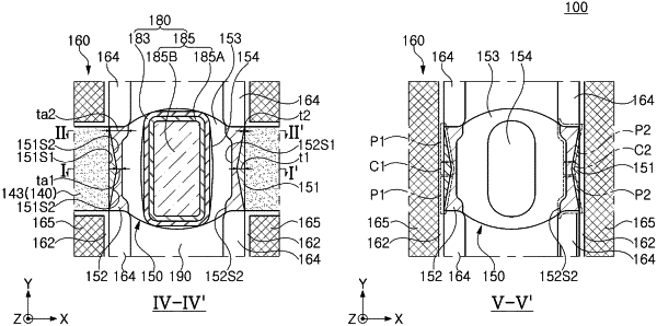
the source/drain region includes a first epitaxial layer on side surfaces of the plurality of channel layers and including a first impurity; a second epitaxial layer on the first epitaxial layer and including the first impurity and a second impurity; and a third epitaxial layer on the second epitaxial layer and including the first impurity,
in a horizontal sectional view of a plane at a height level of one of the plurality of channel layers, the second epitaxial layer includes a peripheral portion having a thickness measured in the first direction that increases along the second direction,
a sum of thicknesses of the first epitaxial layer and the second epitaxial layer is about 2 nm to about 5 nm, and
the second epitaxial layer has a maximum thickness within a range from about 35% to less than 100% of the sum of the thicknesses of the first epitaxial layer and the second epitaxial layer.
|