| CPC H01L 29/7813 (2013.01) [H01L 21/046 (2013.01); H01L 21/765 (2013.01); H01L 29/063 (2013.01); H01L 29/1095 (2013.01); H01L 29/1608 (2013.01); H01L 29/407 (2013.01); H01L 29/66068 (2013.01)] | 11 Claims |

|
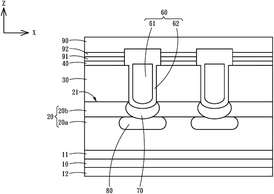
1. A silicon carbide semiconductor device, comprising:
a first silicon carbide semiconductor layer, having a first conductive type;
a second silicon carbide semiconductor layer, having the first conductive type and comprising a drift layer arranged on the first silicon carbide semiconductor layer and a current spreading layer arranged on the drift layer;
a third silicon carbide semiconductor layer, having a second conductive type and arranged on an upper surface of the second silicon carbide semiconductor layer;
a first semiconductor region, having the first conductive type and arranged in the third silicon carbide semiconductor layer;
a trench, vertically penetrating through the first semiconductor region and the third silicon carbide semiconductor layer to the second silicon carbide semiconductor layer and extending along a first horizontal direction;
a second semiconductor region, having the second conductive type, the second semiconductor region comprising a plurality of first portions which extends along a second horizontal direction and being formed in the third silicon carbide semiconductor layer and at least one second portion in the second silicon carbide semiconductor layer below the trench, wherein the first portions and the second portion adjoin each other, and the second semiconductor region surrounds the trench;
a gate region, buried into the trench and comprising a gate insulating layer formed on a wall of the trench and a poly gate formed on the gate insulating layer;
a third semiconductor region, arranged outsides the trench and having the second conductive type, the third semiconductor region comprising a field plate which is at least partially formed in the second silicon carbide semiconductor layer and is between the trench and the second portion of the second semiconductor region, side walls of the field plate are in contact to the current spreading layer;
a shield region, having the second conductive type, the shield region being in the second silicon carbide semiconductor layer below the trench and below the field plate; and
a metal electrode, in contact to the first semiconductor region and the gate region.
|