| CPC H01L 29/1608 (2013.01) [C30B 29/36 (2013.01)] | 10 Claims |
|
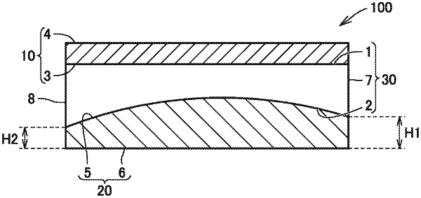
1. A silicon carbide epitaxial substrate comprising:
a silicon carbide substrate having a first main surface and a second main surface opposite to the first main surface;
a first silicon carbide epitaxial layer in contact with a whole of the first main surface; and
a second silicon carbide epitaxial layer in contact with a whole of the second main surface, wherein
a carrier concentration of the silicon carbide substrate is higher than a carrier concentration of each of the first silicon carbide epitaxial layer and the second silicon carbide epitaxial layer;
wherein the silicon carbide substrate does not comprise an epitaxial layer.
|