| CPC H01L 27/156 (2013.01) [H01L 33/0066 (2013.01); H01L 33/0093 (2020.05); H01L 33/24 (2013.01); H01L 33/30 (2013.01); H01L 33/38 (2013.01); H01L 33/44 (2013.01); H01L 2933/0025 (2013.01)] | 20 Claims |
|
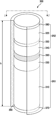
1. A light-emitting diode comprising:
a first semiconductor region having a first conductive type;
a second semiconductor region having a second conductive type; and
an active layer disposed between the first semiconductor region and the second semiconductor region and including phosphorus (P), wherein
the light-emitting diode has a rod shape,
the second semiconductor region includes a first semiconductor layer, a second semiconductor layer, and a third semiconductor layer which are sequentially stacked,
the first semiconductor layer is disposed between the active layer and the second semiconductor layer, and
the second semiconductor layer includes a compound represented by Chemical Formula 1 and satisfying Equation 1,
AlGaInP, Chemical Formula 1
Equation 1:
1/9≤M≤9, wherein M refers to a content of aluminum (Al) with respect to a content of gallium (Ga) included in AlGaInP (i.e., the content of aluminum (Al) in AlGaInP (at. %)/the content of gallium (Ga) in AlGaInP (at. %)).
|