| CPC H01L 27/14634 (2013.01) [H01L 27/14614 (2013.01); H01L 27/14636 (2013.01); H01L 27/14641 (2013.01); H01L 27/14643 (2013.01); H04N 25/76 (2023.01)] | 6 Claims |

|
1. A solid-state imaging element comprising:
a first semiconductor substrate that includes a floating diffusion that temporarily holds an electric signal output from a photoelectric conversion element; and
a second semiconductor substrate that faces the first semiconductor substrate, wherein
the second semiconductor substrate includes:
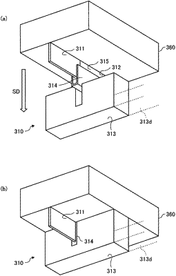
a first transistor disposed on a side facing the first semiconductor substrate, the first transistor including:
a channel extending along a thickness direction of the second semiconductor substrate; and
a multi-gate extending along the thickness direction of the second semiconductor substrate and sandwiching the channel, wherein the multi-gate of the first transistor is connected to the floating diffusion;
a source region that extends from one surface side of the second semiconductor substrate and reaches another surface side of the second semiconductor substrate,
wherein the one surface side of the second semiconductor substrate is opposite the another surface side of the second semiconductor substrate, and
wherein the another surface side of the second semiconductor substrate faces the first semiconductor substrate; and
a drain region that extends from the one surface side of the second semiconductor substrate and reaches the another surface side of the second semiconductor substrate,
wherein the source region is connected to a signal line that transmits the electric signal from the one surface side of the second semiconductor substrate, and
wherein the drain region is connected to a power supply potential from the one surface side of the second semiconductor substrate.
|