| CPC H01L 27/1255 (2013.01) [H01L 27/124 (2013.01); H01L 27/1248 (2013.01)] | 17 Claims |
|
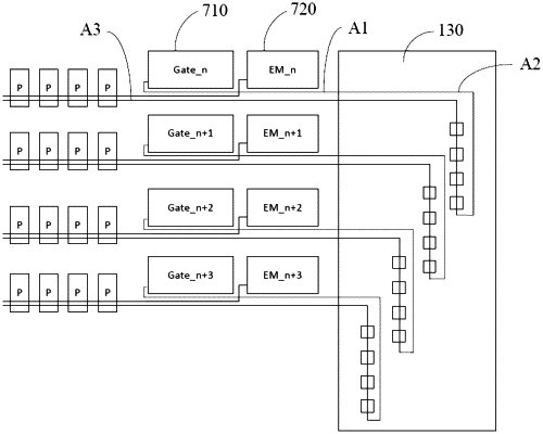
1. A display substrate, comprising a display region and a frame region surrounding the display region, wherein the display region comprises a first region and a second region, and a quantity of sub-pixels connected to each gate line in the first region is less than the quantity of sub-pixels connected to each gate line in the second region; and
the display substrate comprises a signal line arranged in the frame region, an orthogonal projection of each gate line in the first region onto a base substrate of the display substrate partially overlaps an orthogonal projection of the signal line onto the base substrate, and a capacitor is formed between the signal line and the gate line in the first region to increase a load capacitance of the gate line in the first region.
|