| CPC H01L 27/1251 (2013.01) [H01L 27/1259 (2013.01); H01L 29/66742 (2013.01); H01L 29/78618 (2013.01)] | 17 Claims |
|
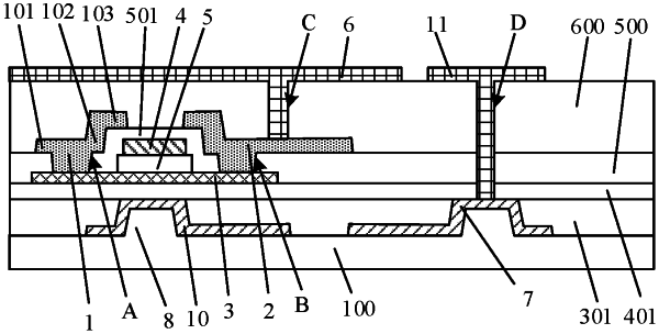
1. A thin-film transistor (TFT) array substrate, comprising a source, a drain, and a first gate; wherein
a protrusive structure is defined between the source and the drain, and the first gate is disposed inside the protrusive structure; and
in a plane where a surface of the first gate is disposed, a sum of an overlapped area of a projection of the source and a projection of the first gate and an overlapped area of a projection of the drain and the projection of the first gate is less than an area threshold,
the TFT array substrate further comprising a substrate and a second gate, wherein the substrate is provided with a boss mated with the second gate, and the second gate covers the boss, wherein the second gate is disposed at a corresponding position on a side, proximal to the substrate, of the protrusive structure, wherein a width of the second gate is less than a width of a channel formed by the source and the drain on an active layer, the second gate is closer to the substrate than the first gate is, orthographic projections of the first gate and the second gate on the substrate are overlapped, a second planarization layer is disposed on the substrate, the second planarization layer does not cover an upper surface of the second gate, and an upper surface of the second planarization layer is flush with the upper surface of the second gate,
the TFT array substrate further comprising a cathode disposed on the substrate, wherein the second gate and the cathode are disposed on a same layer and formed by a same step.
|