| CPC H01L 27/124 (2013.01) [G02F 1/136209 (2013.01); G02F 1/136213 (2013.01); G02F 1/136222 (2021.01); G02F 1/13629 (2021.01); G02F 1/1368 (2013.01); H01L 27/1255 (2013.01)] | 18 Claims |
|
1. An array substrate, comprising:
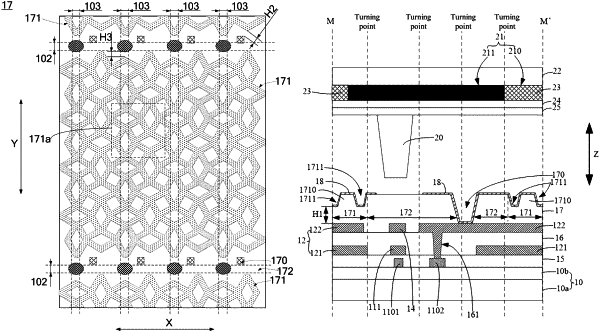
a first substrate (10), comprising a plurality of sub-pixel regions (101) arranged in an array along a row direction (X) and a column direction (Y);
a pixel circuit layer formed on the first substrate (10), comprising a plurality of sub-pixel circuits, wherein at least part of the sub-pixel circuits is located in the sub-pixel regions (101);
a planarization layer (17) formed on the pixel circuit layer, wherein the planarization layer (17) is provided with a first via hole (170) located in the sub-pixel regions (101), and comprises at least one pattern portion (171), the pattern portion (171) comprises a plurality of pattern units (171a) arranged in an array along the row direction (X) and the column direction (Y), and the pattern unit (171a) is uneven and located at least in the sub-pixel regions (101); wherein the pattern unit (171a) comprises a plurality of first bumps (1710) arranged along a circumferential direction (C) of the pattern unit (171a) and an spacing groove (1711) surrounding each of the first bumps (1710), and a part of the spacing groove (1711) is shared by two adjacent first bumps (1710) in the circumferential direction (C); and
a reflective electrode layer formed on the planarization layer (17), wherein the reflective electrode layer comprises a plurality of reflective electrodes (18) that are mutually disconnected, each of the reflective electrodes (18) is located in one of the sub-pixel regions (101) and is electrically connected to the sub-pixel circuit through the first via hole (170), and a portion of the reflective electrode (18) corresponding to the pattern unit (171a) is in an uneven shape matching the pattern unit (171a),
wherein,
the first substrate (10) further comprises multiple rows of first wiring regions (102) and multiple columns of second wiring regions (103), the first wiring regions (102) and each row of sub-pixel regions (101) are alternately arranged in the column direction (Y), and the second wiring regions (103) and each column of the sub-pixel regions (101) are alternately arranged in the row direction (X);
the pixel circuit layer further comprises multiple rows of gate lines (13) and multiple columns of data lines (14), the gate lines (13) are located in the first wiring regions (102), the data lines (14) are located in the second wiring regions (103), and the gate lines (13) and the data lines (14) are respectively electrically connected to the sub-pixel circuit,
the sub-pixel circuit comprises a storage capacitor (12) and a transistor (11);
the storage capacitor (12) is located in the sub-pixel region (101), and comprises a first electrode plate (121) and a second electrode plate (122) that are opposite to each other in a thickness direction (Z) of the first substrate (10), the first electrode plate (121) and the gate line (13) are arranged in a same layer and disconnected from each other, the second electrode plate (122) and the data line (14) are arranged in a same layer and disconnected from each other, and the second electrode plate (122) is connected to the reflective electrode (18) through the first via hole (170);
the transistor (11) comprises an active layer (110), a gate (111), a source (112) and a drain (113); the active layer (110) is located at one side of the gate line (13) near the first substrate (10), and comprises a first active portion (1101) located in the second wiring region (103), a second active portion (1102) opposite to the first active portion (1101) in the row direction (X), and a third active portion (1103) at least located in the sub-pixel region (101); an orthographic projection of the first active portion (1101) on the first substrate (10) at least partially overlaps with an orthographic projection of the gate line (13) on the first substrate (10); a first end of the first active portion (1101) is located at one side of the gate line (13) away from the third active portion (1103), and a second end of the first active portion (1101) is connected to a first end of the third active portion (1103); a first end and a second end of the second active portion (1102) are respectively located in two adjacent sub-pixel regions (101) in the row direction (X), the first end of the second active portion (1102) is located at one side of the gate line (13) away from the third active portion (1103), and the second end of the second active portion (1102) is connected to a second end of the third active portion (1103); and
the gate (111) of the transistor (11) is formed by a part of the gate lines (13) overlapping with the first active portion (1101) and the second active portion (1102) in the thickness direction (Z) of the first substrate (10), the source (112) of the transistor (11) is formed by a part of the data lines (14) overlapping with the first end of the first active portion (1101) in the thickness direction (Z) of the first substrate (10), the source (112) is connected to the first end of the first active portion (1101) through the second via hole (160), the drain (113) of the transistor (11) is formed by a part of the second electrode plate (122) overlapping with the first end of the second active portion (1102) in the thickness direction (Z) of the first substrate (10), and the drain (113) is connected to the first end of the second active portion (1102) through the third via hole (161).
|