| CPC H01L 27/0886 (2013.01) [H01L 21/76232 (2013.01); H01L 21/823821 (2013.01); H01L 21/823878 (2013.01); H01L 27/0924 (2013.01)] | 15 Claims |

|
1. A semiconductor device comprising:
a substrate;
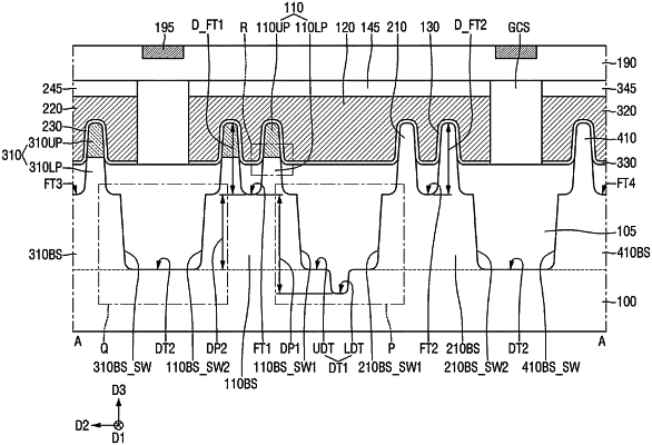
a first base fin protruding from the substrate and extending in a first direction;
a first fin type pattern protruding from the first base fin and extending in the first direction;
a field insulating film on the substrate; and
a gate electrode intersecting the first fin type pattern on the field insulating film, and extending in a second direction that is perpendicular to the first direction,
wherein the first base fin includes a first sidewall and a second sidewall, the first and second sidewalls extending in the first direction, the first sidewall opposite to the second sidewall,
the first sidewall of the first base fin at least partially defines a first deep trench,
the second sidewall of the first base fin at least partially defines a second deep trench,
a depth of the first deep trench is greater than a depth of the second deep trench,
the first fin type pattern includes a lower fin type pattern, and an upper fin type pattern directly connected to the lower fin type pattern, the upper fin type pattern on the lower fin type pattern,
the lower fin type pattern includes the same material as the first base fin,
the lower fin type pattern includes a material different from the upper fin type pattern,
the field insulating film fills the first deep trench and the second deep trench, and covers a part of sidewalls of the first fin type pattern, and
the gate electrode overlaps the upper fin type pattern in a third direction that is perpendicular to the first direction and the second direction.
|