| CPC H01L 27/0207 (2013.01) [H01L 21/84 (2013.01); H01L 27/12 (2013.01); H03K 3/037 (2013.01); H01L 2027/11861 (2013.01); H01L 2027/11866 (2013.01); H01L 2027/11887 (2013.01)] | 20 Claims |
|
1. A method, comprising:
forming a plurality of power rails in a first layer, wherein the plurality of power rails extend in a first direction and are separated from each other in a second direction;
forming a plurality of conductive lines in a second layer over the first layer, wherein the plurality of conductive lines extend in the second direction;
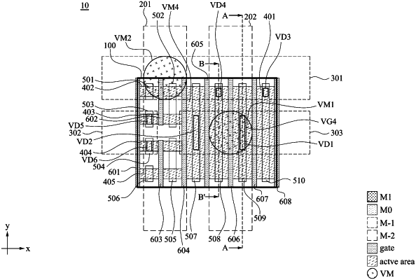
forming a plurality of active areas in a third layer over the second layer;
forming a plurality of conductive segments over the plurality of active areas in the third layer, wherein a first active area of the plurality of active areas is coupled to at least a first conductive line and a second conductive line of the plurality of conductive lines;
forming a plurality of gates above the plurality of active areas and interposed between the plurality of conductive segments;
forming a plurality of conductive traces in a fourth layer above the third layer, wherein the plurality of conductive traces extend in the second direction; and
forming a conductive pattern in a fifth layer above the fourth layer, wherein the conductive pattern is coupled to the plurality of conductive traces.
|