| CPC H01L 25/0753 (2013.01) [H01L 33/10 (2013.01); H01L 33/58 (2013.01); H01L 33/62 (2013.01)] | 14 Claims |
|
1. A multi-pixel display device, comprising:
an integrated circuit,
a plurality of light-emitting semiconductor chips disposed on the integrated circuit,
a display area having a plurality of pixels, each of the light-emitting semiconductor chips being associated with one of the plurality of pixels,
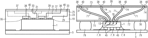
a light-directing element disposed between the plurality of light-emitting semiconductor chips and the display area and adapted to direct light of each light-emitting semiconductor chip from the plurality of light-emitting semiconductor chips to its associated pixel,
wherein
the associated pixel to which the light is directed is arranged laterally offset above the light-emitting semiconductor chip associated therewith,
the light-directing element having a top side and a bottom side comprises a plurality of light-guiding structures each having an in-coupling area at the bottom side and an out-coupling area at the top side to the associated pixel, and
the light-emitting semiconductor chip is arranged overlapped to the in-coupling area of the light guiding structure comprising the out-coupling area to the associated pixel.
|