| CPC H01L 25/0655 (2013.01) [H01L 23/3121 (2013.01); H01L 23/49811 (2013.01); H01L 25/50 (2013.01); H03F 3/213 (2013.01); H03F 2200/451 (2013.01)] | 20 Claims |
|
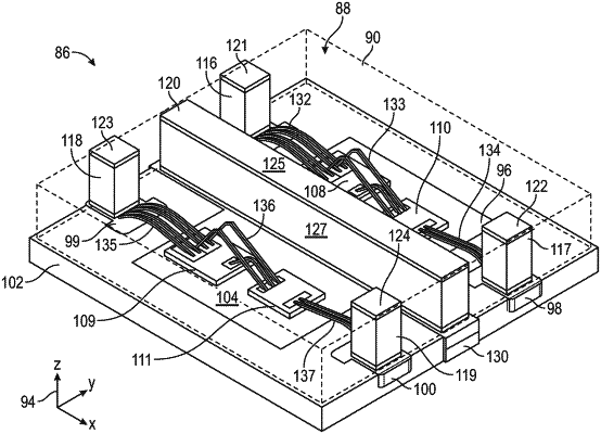
1. A leadless power amplifier (PA) package, comprising:
a base flange having a die mount surface and a lower flange surface located opposite the die mount surface in a package height direction;
a first set of interposer mount pads spaced from the base flange;
a first radio frequency (RF) power die attached to the die mount surface of the base flange and electrically interconnected with the first set of interposer mount pads;
a topside termination interposer (TTI) arrangement electrically coupled to the first set of interposer mount pads and projecting therefrom in the package height direction;
a package body enclosing the first RF power die and having a package topside surface opposite the lower flange surface, the package topside surface extending substantially parallel to the die mount surface; and
topside input/output (I/O) terminals accessible from the package topside surface and electrically interconnected with the first RF power die through the TTI arrangement and through the first set of interposer mount pads.
|