| CPC H01L 25/0652 (2013.01) [H01L 21/67098 (2013.01); H01L 23/34 (2013.01); H01L 23/4012 (2013.01); H01L 2225/06589 (2013.01)] | 11 Claims |

|
1. A method for managing thermal energy, comprising:
applying thermal energy from a thermal component to a first set of stacked semiconductor devices of a semiconductor device assembly; and
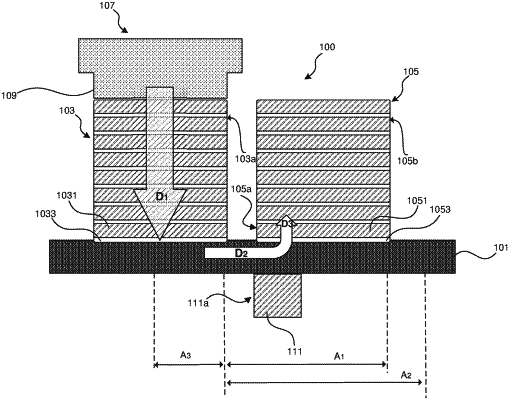
absorbing, by a temperature adjusting component of the semiconductor device assembly, at least a portion of thermal energy generated by the thermal component such that the portion of thermal energy is inhibited from increasing a temperature of a second set of stacked semiconductor devices based at least in part on the temperature adjusting component contacting a substrate of the semiconductor device assembly on a side opposite the second set of stacked semiconductor devices in a region at least partially vertically aligned with the second set of stacked semiconductor devices and excluding any region vertically aligned with the first set of stacked semiconductor devices.
|