| CPC H01L 25/0652 (2013.01) [H01L 23/13 (2013.01); H01L 25/18 (2013.01); H01L 2225/0651 (2013.01); H01L 2225/06517 (2013.01); H01L 2225/06558 (2013.01); H01L 2225/06562 (2013.01); H01L 2225/06586 (2013.01)] | 10 Claims |
|
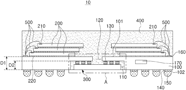
1. A semiconductor package comprising:
a package substrate having a first surface having a plurality of first connection pads, a second surface that is opposite the first surface and having a concave portion and ball lands disposed in a peripheral region of the concave portion, a through-hole passing through the first surface and the second surface on a bottom surface of the concave portion, and a plurality of second connection pads disposed in a peripheral region of the through-hole on the bottom surface;
at least one first semiconductor chip mounted on the first surface and electrically connected to the plurality of first connection pads;
at least one second semiconductor chip mounted on the bottom surface of the concave portion and electrically connected to the plurality of second connection pads; and
external terminals respectively attached to the ball lands.
|