| CPC H01L 25/0652 (2013.01) [H01L 21/76898 (2013.01); H01L 23/481 (2013.01); H01L 24/08 (2013.01); H01L 24/80 (2013.01); H01L 24/94 (2013.01); H01L 25/50 (2013.01); H01L 2224/08146 (2013.01); H01L 2224/80895 (2013.01); H01L 2225/06513 (2013.01); H01L 2225/06524 (2013.01); H01L 2225/06527 (2013.01); H01L 2225/06544 (2013.01); H01L 2225/06555 (2013.01); H01L 2225/06586 (2013.01)] | 20 Claims |

|
1. A semiconductor package comprising:
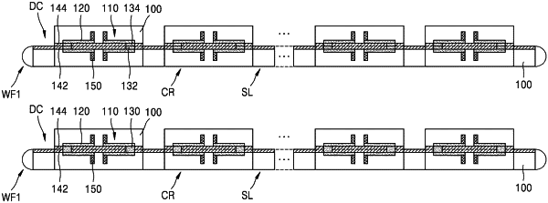
a first device layer including a first semiconductor substrate having a first active surface, a first cover insulating layer covering the first active surface of the first semiconductor substrate, and a plurality of first through-electrodes passing through at least a portion of the first semiconductor substrate, the first semiconductor substrate comprising a plurality of first semiconductor chip regions, each of the plurality of first semiconductor chip regions provided with at least one first semiconductor device on the first active surface of the first semiconductor substrate;
a second device layer including a second semiconductor substrate having a second active surface, a second cover insulating layer covering the second active surface of the second semiconductor substrate, and a plurality of second through-electrodes passing through at least a portion of the second semiconductor substrate, the second semiconductor substrate comprising a plurality of second semiconductor chip regions, each of the plurality of second semiconductor chip regions provided with at least one second semiconductor device on the second active surface of the second semiconductor substrate, the plurality of second semiconductor chip regions vertically overlapping the plurality of first semiconductor chip regions, respectively, the second cover insulating layer in contact with the first cover insulating layer;
a third device layer including an upper semiconductor chip, the upper semiconductor chip including a plurality of chip connection pads and vertically overlapping at least two of the plurality of first semiconductor chip regions and vertically overlapping at least two of the plurality of second semiconductor chip regions;
a plurality of device bonded pads passing through the first cover insulating layer and the second cover insulating layer, the plurality of device bonded pads electrically connecting the plurality of first through-electrodes and the plurality of second through-electrodes to the upper semiconductor chip; and
a rewiring structure on a first surface of the first device layer, the first surface of the first device layer being opposite to a second surface of the first device layer that faces the second device layer, the rewiring structure including,
a plurality of rewiring insulating layers,
a plurality of rewiring conductive patterns each on one of top surfaces or bottom surfaces of one of the plurality of rewiring insulating layers, and
a plurality of rewiring via patterns each connecting a vertically neighboring pair of the plurality of rewiring conductive patterns and passing through at least one of the plurality of rewiring insulating layers; and
a plurality of external connection terminals contacting the plurality of rewiring conductive patterns and electrically connected to the plurality of first through-electrodes,
wherein the plurality of rewiring conductive patterns include first rewiring conductive patterns being arranged at a first pitch and second rewiring conductive patterns being arranged at a second pitch greater the first pitch, and
wherein the second rewiring conductive patterns are closer to the plurality of external connection terminals than the first rewiring conductive patterns.
|