| CPC H01L 24/92 (2013.01) [H01L 21/56 (2013.01); H01L 23/49527 (2013.01); H01L 23/49575 (2013.01); H01L 23/52 (2013.01); H01L 24/24 (2013.01); H01L 24/29 (2013.01); H01L 24/32 (2013.01); H01L 24/40 (2013.01); H01L 24/73 (2013.01); H01L 24/82 (2013.01); H01L 24/83 (2013.01); H01L 24/84 (2013.01); H01L 23/3107 (2013.01); H01L 23/49513 (2013.01); H01L 2224/24011 (2013.01); H01L 2224/24101 (2013.01); H01L 2224/24105 (2013.01); H01L 2224/24137 (2013.01); H01L 2224/24246 (2013.01); H01L 2224/29139 (2013.01); H01L 2224/32245 (2013.01); H01L 2224/40101 (2013.01); H01L 2224/40137 (2013.01); H01L 2224/73213 (2013.01); H01L 2224/73217 (2013.01); H01L 2224/73263 (2013.01); H01L 2224/73267 (2013.01); H01L 2224/82101 (2013.01); H01L 2224/8384 (2013.01); H01L 2224/8484 (2013.01); H01L 2224/92142 (2013.01); H01L 2224/92144 (2013.01)] | 20 Claims |
|
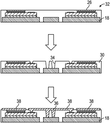
1. A semiconductor package comprising:
a metal layer;
two or more die, each of the two or more die coupled to the metal layer at a drain of each of the two or more die, the two or more die and the metal layer arranged in two parallel planes;
a first interconnect layer coupled at a source of each of the two or more die;
a second interconnect layer electrically coupled to a gate of each of the two or more die and to a gate package contact through one or more vias; and
an encapsulant that encapsulates the two or more die and at least a portion of the first interconnect layer, the metal layer, and the second interconnect layer;
wherein each drain of the two or more die faces towards the metal layer.
|