| CPC H01L 24/14 (2013.01) [H01L 23/5226 (2013.01); H01L 2224/13008 (2013.01); H01L 2224/13009 (2013.01); H01L 2224/13166 (2013.01); H01L 2224/13171 (2013.01); H01L 2224/13184 (2013.01); H01L 2224/16146 (2013.01)] | 20 Claims |
|
1. A semiconductor package comprising:
a first sub-package including a first semiconductor chip;
a second sub-package disposed on the first sub-package and including a second semiconductor chip; and
an inter-package connection structure connecting the first sub-package to the second sub-package,
wherein each of the first sub-package and the second sub-package comprises
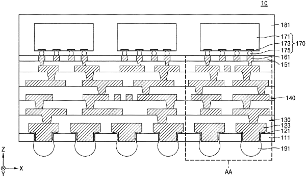
a lower redistribution layer structure,
a bump pad disposed under the lower redistribution layer structure, the bump pad having an upper structure of a first width and a lower structure of a second width less than the first width,
a metal seed layer disposed along a lower surface of the upper structure and a side surface of the lower structure,
a lower insulating layer surrounding the lower redistribution layer structure and the bump pad, and
a bump structure disposed under the bump pad,
wherein a first undercut is disposed at one end of the metal seed layer that contacts the upper structure and a second undercut is disposed at an other end of the metal seed layer that contacts the lower structure, and
wherein the first semiconductor chip and the second semiconductor chip include different types of semiconductor chips.
|