| CPC H01L 24/02 (2013.01) [H01L 21/486 (2013.01); H01L 23/49838 (2013.01); H01L 23/544 (2013.01); H01L 24/03 (2013.01); H01L 24/05 (2013.01); H01L 24/06 (2013.01); H01L 25/105 (2013.01); H01L 25/18 (2013.01); H01L 23/481 (2013.01); H01L 23/49816 (2013.01); H01L 23/49827 (2013.01); H01L 24/04 (2013.01); H01L 2223/54426 (2013.01); H01L 2224/0213 (2013.01); H01L 2224/02141 (2013.01); H01L 2224/02145 (2013.01); H01L 2224/0215 (2013.01); H01L 2224/03019 (2013.01); H01L 2224/03462 (2013.01); H01L 2224/0401 (2013.01); H01L 2224/05019 (2013.01); H01L 2224/05025 (2013.01); H01L 2224/05082 (2013.01); H01L 2224/0603 (2013.01); H01L 2224/06182 (2013.01)] | 20 Claims |
|
1. An interposer comprising:
a base layer having opposite first and second surfaces;
a wiring structure on the first surface of the base layer;
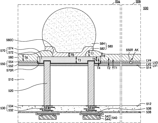
an interposer protective layer disposed on the second surface of the base layer and having a pad recess with a lower surface of the interposer protective layer at a first vertical level and a bottom surface of the pad recess at a second vertical level that is higher than the first vertical level, the interposer protective layer comprising a lower interposer protective layer covering the second surface of the base layer; and an upper interposer protective layer formed of a material that is different from that of the lower interposer protective layer and has a lower surface in contact with the lower interposer protective layer at a third vertical level and an upper surface positioned at a fourth vertical level that is higher than the third vertical level;
an interposer pad of which a portion fills the pad recess of the interposer protective layer and the remaining portion protrudes from the upper surface of the upper interposer protective layer; and
an interposer through electrode extending through the base layer and the interposer protective layer to the interposer pad, the interposer through electrode electrically connecting the wiring structure to the interposer pad.
|