| CPC H01L 23/645 (2013.01) [H01L 21/4853 (2013.01); H01L 21/565 (2013.01); H01L 23/3128 (2013.01); H01L 23/49838 (2013.01); H01L 24/16 (2013.01); H01L 28/10 (2013.01); H01L 2224/16227 (2013.01); H01L 2924/19042 (2013.01); H01L 2924/19103 (2013.01)] | 10 Claims |
|
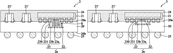
1. A method of manufacturing an electronic package, comprising:
providing an electronic component having a first conductive layer and a carrier having a second conductive layer; and
disposing the electronic component on the carrier via a plurality of conductive bumps with at least one magnetically permeable member interposed between the electronic component and the carrier, wherein the plurality of conductive bumps are electrically connected with the first conductive layer and the second conductive layer, and the magnetically permeable member is located between the first conductive layer and the second conductive layer.
|