| CPC H01L 23/535 (2013.01) [H10B 41/27 (2023.02); H10B 41/41 (2023.02); H10B 43/27 (2023.02); H10B 43/40 (2023.02); H01L 25/18 (2013.01)] | 20 Claims |

|
1. A semiconductor device, comprising:
a lower structure including a peripheral circuit;
a stack structure including interlayer insulating layers and horizontal layers alternately stacked on the lower structure;
a vertical memory structure penetrating through the stack structure in a vertical direction;
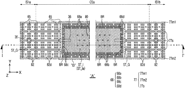
a first barrier structure and a second barrier structure penetrating through the stack structure in the vertical direction and parallel to each other;
a supporter pattern penetrating through the stack structure in the vertical direction and spaced apart from the first and second barrier structures; and
through contact plugs penetrating through the stack structure in the vertical direction between the first and second barrier structures, wherein:
the first barrier structure includes first barrier patterns arranged in a first direction and spaced apart from each other, and second barrier patterns arranged in the first direction and spaced apart from each other,
each of the first and second barrier patterns includes a linear shape extending in the first direction, and
in a first barrier pattern and a second barrier pattern adjacent to each other among the first and second barrier patterns, a portion of the first barrier pattern opposes a portion of the second barrier pattern in a second direction perpendicular to the first direction.
|