| CPC H01L 23/5226 (2013.01) [H01L 23/5385 (2013.01); H01L 24/06 (2013.01); H01L 24/14 (2013.01); H01L 25/0655 (2013.01); H01L 25/50 (2013.01); H01L 21/563 (2013.01); H01L 24/05 (2013.01); H01L 24/13 (2013.01); H01L 25/18 (2013.01); H01L 2224/0401 (2013.01); H01L 2224/05541 (2013.01); H01L 2224/05568 (2013.01); H01L 2224/0603 (2013.01); H01L 2224/131 (2013.01); H01L 2224/1403 (2013.01); H01L 2224/16225 (2013.01); H01L 2224/16227 (2013.01); H01L 2224/83102 (2013.01); H01L 2924/12042 (2013.01); H01L 2924/15192 (2013.01)] | 20 Claims |
|
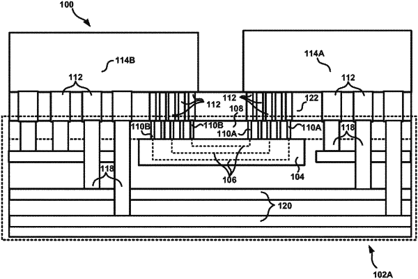
1. An apparatus, comprising:
a medium having an interconnect in an insulating layer, the interconnect above a conductive line;
an interconnect element above the medium, the interconnect element having electrically conductive pads thereon, and the interconnect element comprising a silicon die, wherein the interconnect element is vertically over and spaced apart from the conductive line of the medium;
a conductive structure laterally spaced apart from the interconnect element, the conductive structure vertically over and electrically coupled to the interconnect of the medium;
an insulator material on the insulating layer of the medium, the insulator material laterally adjacent to the interconnect element, and the insulator material in lateral contact with the conductive structure, wherein the insulator material is vertically over and spaced apart from the conductive line of the medium;
a first die over the interconnect element, the first die coupled to a first of the electrically conductive pads of the interconnect element, and the first die electrically coupled to the conductive structure; and
a second die over the interconnect element, the second die coupled to a second of the electrically conductive pads of the interconnect element.
|