| CPC H01L 23/5226 (2013.01) [H01L 21/76805 (2013.01); H01L 21/7682 (2013.01); H01L 21/76895 (2013.01); H01L 23/5283 (2013.01); H01L 23/5329 (2013.01); H01L 23/535 (2013.01); H10B 41/27 (2023.02); H10B 43/27 (2023.02)] | 10 Claims |
|
1. A semiconductor structure, comprising:
semiconductor devices located over a substrate;
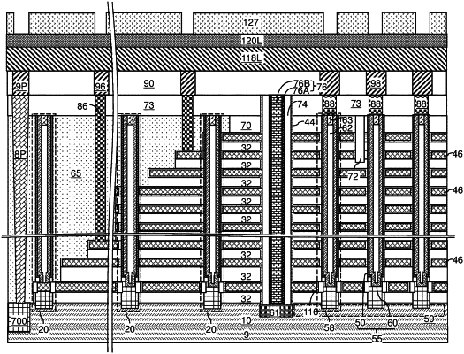
bit lines electrically connected to the semiconductor devices and having a respective reentrant vertical cross-sectional profile within a vertical plane that is perpendicular to a lengthwise direction along which the bit lines laterally extend;
dielectric rails that are interlaced with the bit lines along a horizontal direction that is perpendicular to the lengthwise direction; and
dielectric cap strips located on top surface of the dielectric rails and covering peripheral regions of the top surfaces of the bit lines and not covering middle regions of the top surfaces of the bit lines;
wherein top surfaces of the dielectric rails are located within a horizontal plane including top surfaces of the bit lines; and
wherein lengthwise edges of the dielectric cap strips are laterally offset by a lateral offset distance from a most proximal lengthwise top edge of lengthwise top edges of the bit lines.
|
|
3. A semiconductor structure, comprising:
semiconductor devices located over a substrate;
bit lines electrically connected to the semiconductor devices and having a respective reentrant vertical cross-sectional profile within a vertical plane that is perpendicular to a lengthwise direction along which the bit lines laterally extend;
dielectric rails that are interlaced with the bit lines along a horizontal direction that is perpendicular to the lengthwise direction; and
dielectric cap strips located on top surface of the dielectric rails and covering peripheral regions of the top surfaces of the bit lines and not covering middle regions of the top surfaces of the bit lines;
wherein top surfaces of the dielectric rails are located within a horizontal plane including top surfaces of the bit lines; and
wherein each of the dielectric cap strips has a pair of convex top surface segments that are adjoined to a planar top surface segment and laterally extend along the lengthwise direction.
|
|
4. A semiconductor structure, comprising:
semiconductor devices located over a substrate;
bit lines electrically connected to the semiconductor devices and having a respective reentrant vertical cross-sectional profile within a vertical plane that is perpendicular to a lengthwise direction along which the bit lines laterally extend;
dielectric rails that are interlaced with the bit lines along a horizontal direction that is perpendicular to the lengthwise direction;
dielectric cap strips located on top surface of the dielectric rails and covering peripheral regions of the top surfaces of the bit lines and not covering middle regions of the top surfaces of the bit lines;
a via-level dielectric layer overlying the dielectric cap strips; and
a bit-line-contact via structure vertically extending through the via-level dielectric layer and contacting a top surface of one of the bit lines;
wherein the bit-line-contact via structure comprises a straight sidewall segment in contact with the via-level dielectric layer and a pair of concave sidewall segments in contact with convex sidewall segments of a pair of dielectric cap strips of the dielectric cap strips.
|
|
5. A semiconductor structure, comprising:
semiconductor devices located over a substrate;
bit lines electrically connected to the semiconductor devices and having a respective reentrant vertical cross-sectional profile within a vertical plane that is perpendicular to a lengthwise direction along which the bit lines laterally extend;
dielectric rails that are interlaced with the bit lines along a horizontal direction that is perpendicular to the lengthwise direction; and
dielectric cap strips located on top surface of the dielectric rails and covering peripheral regions of the top surfaces of the bit lines and not covering middle regions of the top surfaces of the bit lines;
wherein each of the reentrant vertical cross-sectional profiles has a lower taper region in which a width of a respective bit line decreases with a vertical distance from the substrate, a reverse-taper region in which the width of the respective bit line increases with the vertical distance from the substrate, and an upper taper region in which the width of the respective bit line decreases with the vertical distance from the substrate.
|
|
10. A semiconductor structure, comprising:
semiconductor devices located over a substrate;
bit lines electrically connected to the semiconductor devices and having a respective reentrant vertical cross-sectional profile within a vertical plane that is perpendicular to a lengthwise direction along which the bit lines laterally extend;
dielectric rails that are interlaced with the bit lines along a horizontal direction that is perpendicular to the lengthwise direction; and
dielectric cap strips located on top surface of the dielectric rails and covering peripheral regions of the top surfaces of the bit lines and not covering middle regions of the top surfaces of the bit lines;
wherein the dielectric rails comprise solid dielectric rails containing no air gaps.
|