| CPC H01L 23/5226 (2013.01) [H01L 23/535 (2013.01); H10B 41/27 (2023.02); H10B 43/27 (2023.02)] | 5 Claims |
|
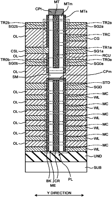
1. A semiconductor memory device comprising:
a plurality of first conductive layers stacked on a substrate;
a plurality of second conductive layers each stacked between the first conductive layers;
a pillar that extends in a stacking direction of the plurality of first conductive layers and the plurality of second conductive layers and forms a plurality of memory cells at intersections of the plurality of first conductive layers and the plurality of second conductive layers in a region where the plurality of first conductive layers and the plurality of second conductive layers are arranged;
a first contact plug that extends in the stacking direction of the plurality of first conductive layers and the plurality of second conductive layers and is connected to the plurality of first conductive layers in the region where the plurality of first conductive layers and the plurality of second conductive layers are arranged; and
a second contact plug that extends in the stacking direction of the plurality of first conductive layers and the plurality of second conductive layers and is connected to the plurality of second conductive layers in the region where the plurality of first conductive layers and the plurality of second conductive layers are arranged.
|