| CPC H01L 23/5226 (2013.01) [H01L 21/4853 (2013.01); H01L 21/486 (2013.01); H01L 21/563 (2013.01); H01L 23/31 (2013.01); H01L 24/14 (2013.01)] | 6 Claims |
|
1. An electronic package, comprising:
an encapsulating layer including a first surface and a second surface opposite to each other;
an electronic structure embedded in the encapsulating layer and comprising:
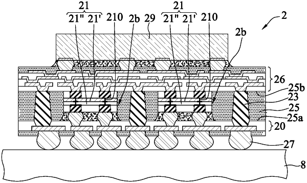
an electronic body including a first side and a second side opposite to each other, wherein the electronic body includes a base of silicon material and a circuit portion formed on the base, such that the base defines the second side, and the circuit portion defines the first side, and the base includes a plurality of conductive through silicon vias as conductive vias electrically connected with the circuit portion and exposed from the second side, wherein the circuit portion includes at least one passivation layer being in direct contact with the base and a circuit layer bonded to the passivation layer and electrically connected with the conductive vias, and wherein the conductive vias are free from extending into the passivation layer;
a plurality of metal pillars as first conductors formed on the first side of the electronic body and electrically connected with the circuit portion;
a plurality of metal pillars as second conductors formed on the second side of the electronic body and electrically connected with the conductive vias;
a first insulating layer formed on the first side of the electronic body and encapsulating the first conductors; and
a second insulating layer formed on the second side of the electronic body and encapsulating the second conductors, wherein the first insulating layer, the second insulating layer, the plurality of first conductors and the plurality of second conductors are located in the encapsulating layer; and
a plurality of conductive pillars embedded in the encapsulating layer.
|