US 11,984,388 B2
Semiconductor package structures and methods of manufacture
Stephen St. Germain, Gilbert, AZ (US); Jay A. Yoder, Phoenix, AZ (US); Dennis Lee Conner, Peoria, AZ (US); Frank Robert Cervantes, Laveen, AZ (US); and Andrew Celaya, Phoenix, AZ (US)
Assigned to SEMICONDUCTOR COMPONENTS INDUSTRIES, LLC, Scottsdale, AZ (US)
Filed by SEMICONDUCTOR COMPONENTS INDUSTRIES, LLC, Scottsdale, AZ (US)
Filed on Jun. 6, 2023, as Appl. No. 18/330,133.
Application 18/330,133 is a division of application No. 17/457,148, filed on Dec. 1, 2021, granted, now 11,710,686.
Application 17/457,148 is a continuation of application No. 16/554,980, filed on Aug. 29, 2019, granted, now 11,217,515, issued on Jan. 4, 2022.
Application 16/554,980 is a continuation in part of application No. 15/833,533, filed on Dec. 6, 2017, granted, now 10,522,448, issued on Dec. 31, 2019.
Application 15/833,533 is a continuation of application No. 15/391,960, filed on Dec. 28, 2016, granted, now 9,870,986, issued on Jan. 16, 2018.
Application 15/391,960 is a continuation of application No. 14/484,141, filed on Sep. 11, 2014, granted, now 9,558,968, issued on Jan. 31, 2017.
Prior Publication US 2023/0317576 A1, Oct. 5, 2023
Int. Cl. H01L 23/498 (2006.01); H01L 21/56 (2006.01); H01L 23/31 (2006.01); H01L 23/495 (2006.01)
CPC H01L 23/49805 (2013.01) [H01L 21/568 (2013.01); H01L 23/3107 (2013.01); H01L 23/49524 (2013.01); H01L 23/49562 (2013.01); H01L 23/49575 (2013.01); H01L 23/49811 (2013.01); H01L 23/49861 (2013.01); H01L 2924/0002 (2013.01); H01L 2924/181 (2013.01)] 20 Claims
OG exemplary drawing
 
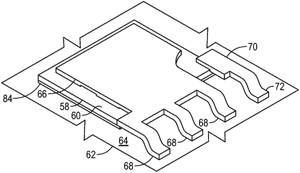
1. A no tie-bar semiconductor package, comprising:
one or more semiconductor die at least partially encapsulated within an encapsulant, the one or more semiconductor die comprising a plurality of electrical contacts;
a plurality of pins exposed through the encapsulant; and
a plurality of electrical connectors fully encapsulated within the encapsulant and electrically interconnecting one or more of the plurality of pins with one or more of the plurality of electrical contacts;
wherein the semiconductor package comprises a flat no-leads semiconductor package;
wherein none of the semiconductor die are coupled with any pins of the plurality of pins through a tie-bar.