| CPC H01L 23/49575 (2013.01) [H01L 23/4952 (2013.01); H01L 23/49562 (2013.01); H01L 23/49568 (2013.01); H01L 24/14 (2013.01); H01L 24/17 (2013.01); H01L 25/0657 (2013.01); H01L 25/074 (2013.01); H01L 29/66431 (2013.01); H01L 29/66462 (2013.01); H01L 29/778 (2013.01); H01L 2924/1033 (2013.01); H01L 2924/13064 (2013.01); H01L 2924/13091 (2013.01)] | 10 Claims |
|
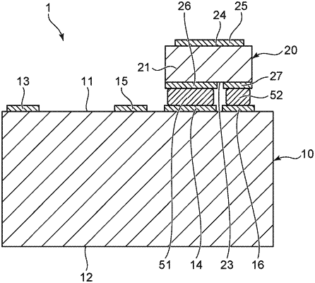
1. A semiconductor device, comprising:
a first chip of a first type, the first chip including
a first surface,
a second surface at a side opposite to the first surface,
a first semiconductor layer including a nitride semiconductor layer of a first conductivity type,
a first electrode pad located at the first surface,
a second electrode pad located at the first surface,
a first gate pad located at the first surface, and
a third electrode pad located at the first surface; and
a second chip located on the first surface of the first chip, the second chip being of a second type that is different from the first type, the second chip including
a third surface facing the first surface of the first chip,
a fourth surface at a side opposite to the third surface,
a second semiconductor layer including a channel of a second conductivity type,
a fourth electrode pad located at the fourth surface,
a fifth electrode pad located at the third surface and bonded to the second electrode pad of the first chip, and
a second gate pad located at the third surface and bonded to the third electrode pad of the first chip.
|