| CPC H01L 23/481 (2013.01) [H01L 23/5383 (2013.01); H01L 24/19 (2013.01); H01L 24/24 (2013.01); H01L 2224/24137 (2013.01); H01L 2924/1431 (2013.01); H01L 2924/1434 (2013.01)] | 13 Claims |
|
1. An electronic circuit comprising:
an integrated circuit die comprising a first substrate, the first substrate supporting:
a first set of contacts,
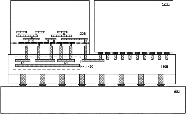
a buried power rail (BPR) disposed within the first substrate, the BPR configured to provide a supply voltage to a plurality of transistors of the integrated circuit die,
a plurality of through-silicon vias (TSV), each TSV of the plurality of TSVs having a first end coupled to the BPR, and a second end coupled to a contact of the first set of contacts, the plurality of TSVs configured to provide the supply voltage to multiple locations within the BPR; and
an interposer comprising a second substrate, the second substrate supporting:
a second set of contacts, each contact of the second set of contacts corresponding to a contact of the first set of contacts, and
a power delivery network (PDN), the PDN coupled to the second set of contacts, the PDN for routing the power supply voltage to the second set of contacts to provide the power supply to each of the TSVs of the integrated circuit die.
|