| CPC H01L 23/3675 (2013.01) [H01L 23/055 (2013.01); H01L 23/3121 (2013.01); H01L 23/42 (2013.01); H01L 23/49822 (2013.01); H01L 23/49827 (2013.01); H01L 24/16 (2013.01); H01L 25/18 (2013.01); H05K 1/111 (2013.01); H05K 1/115 (2013.01); H05K 1/181 (2013.01); H01L 2224/16227 (2013.01)] | 20 Claims |

|
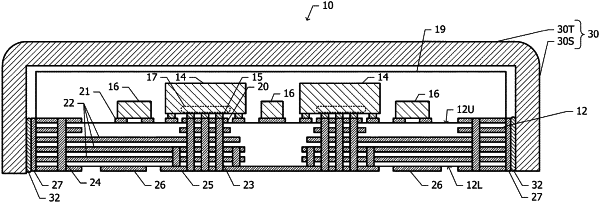
1. A semiconductor package comprising:
a module substrate having a top surface and a bottom surface facing in opposite directions;
a semiconductor chip provided with a plurality of bumps and mounted on the top surface of the module substrate via the bumps; and
a metal member having a top portion and a side portion, the top portion being disposed at a level higher than the semiconductor chip with reference to the top surface of the module substrate, the top portion including the semiconductor chip in plan view, the side portion extending from the top portion toward the module substrate, wherein
the module substrate includes a first metal film disposed on or in at least one of the bottom surface and an internal layer of the module substrate,
the first metal film is electrically connected to the bumps and reaches a side surface of the module substrate, and
the side portion is thermally coupled to the first metal film at the side surface of the module substrate.
|