| CPC H01L 21/823462 (2013.01) [H01L 27/088 (2013.01)] | 20 Claims |
|
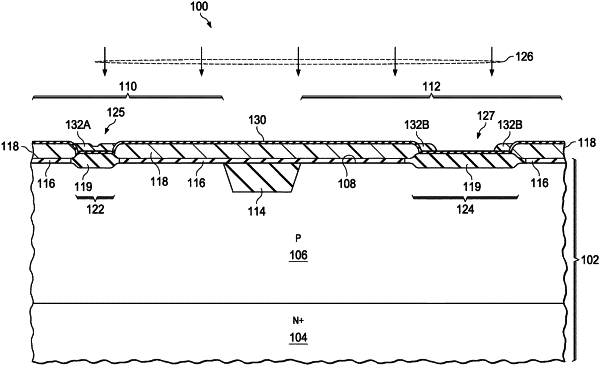
1. A method of fabricating an integrated circuit, comprising:
forming a first opening having a first width and a second opening having a second width in a first dielectric layer over a silicon substrate, the openings exposing the silicon substrate;
oxidizing the exposed silicon substrate to form first and second local oxidation of silicon (LOCOS) structures having a first thickness, the first and second LOCOS structures including bird's beaks;
forming a polysilicon layer over the silicon substrate, the polysilicon layer filling the first and second openings;
performing a blanket etch of the polysilicon layer, wherein the first width is less than a minimum width above which the silicon substrate is exposed in the first opening, by the blanket etch, and the second width is greater than the minimum width, thereby removing at least a portion of the polysilicon layer over the second LOCOS structure while leaving the first LOCOS structure protected by the polysilicon layer; and
further oxidizing the silicon substrate under the second LOCOS structure such that the second LOCOS structure has a second thickness greater than the first thickness.
|