| CPC H01L 21/8222 (2013.01) [H01L 21/31056 (2013.01); H01L 21/8249 (2013.01); H01L 27/0664 (2013.01); H01L 29/66174 (2013.01); H01L 29/66242 (2013.01); H01L 29/7371 (2013.01); H01L 29/93 (2013.01)] | 12 Claims |
|
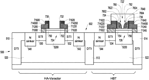
1. A method, comprising jointly producing a bipolar transistor and a variable capacitance diode on a common substrate, wherein jointly producing comprises:
forming an insulating layer over the common substrate;
forming a conductive layer over the insulating layer;
forming a first opening extending through the conductive and insulating layers;
forming a second opening extending through the conductive and insulating layers;
simultaneously forming an intrinsic base of the bipolar transistor and a diode node of the variable capacitance diode;
wherein simultaneously forming comprises forming the diode node of the variable capacitance diode in the first opening at the insulating layer and forming the intrinsic base of the bipolar transistor in the second opening at the insulating layer;
depositing a sacrificial layer over the diode node of the variable capacitance diode and over the intrinsic base of the bipolar transistor;
forming spacers from the deposited sacrificial layer within the second opening over the intrinsic base of the bipolar transistor; and
then forming an emitter of the bipolar transistor over the intrinsic base while the diode node of the variable capacitance diode is covered by the sacrificial layers;
wherein the emitter of the bipolar transistor is positioned between the spacers and in contact with the intrinsic base.
|