| CPC H01L 21/76877 (2013.01) [H01L 21/76831 (2013.01); H01L 23/5223 (2013.01); H01L 23/5226 (2013.01); H01L 23/5283 (2013.01); H01L 28/60 (2013.01)] | 16 Claims |

|
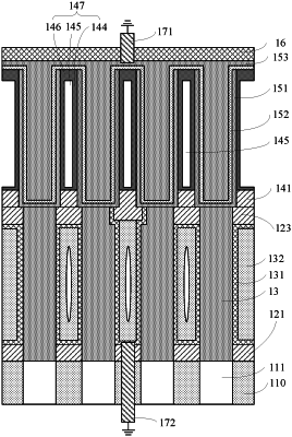
1. A semiconductor structure, comprising:
a substrate, the substrate being provided with a conductive structure;
a first lower electrode and a second lower electrode sequentially stacked, the first lower electrode being located between the second lower electrode and the substrate, the first lower electrode being columnar, the second lower electrode being in a shape of a recess, and the first lower electrode being electrically connected to the conductive structure;
a first dielectric layer and a first upper electrode, the first dielectric layer covering a sidewall surface of the first lower electrode, and the first upper electrode being located on one side of the first dielectric layer away from the first lower electrode;
a second dielectric layer and a second upper electrode, the second dielectric layer covering an inner wall and a bottom surface of the second lower electrode, and the second upper electrode filling the recess of the second lower electrode; and
a support layer comprising a first support layer, a second support layer, the first support layer being located between bottoms of the first lower electrodes, the second support layer being located between tops of the first lower electrodes, and the second support layer between tops of the first lower electrodes having a different dimension along the direction of the surface of the substrate, wherein the second support layer between the tops of the first lower electrodes having a larger dimension along the direction of the surface of the substrate is in direct contact with the first upper electrode therebelow; and the second support layer between the tops of the first lower electrodes having a smaller dimension along the direction of the surface of the substrate is in direct contact with the first dielectric layer therebelow.
|