| CPC H01L 21/76832 (2013.01) [H01L 21/76831 (2013.01); H01L 28/88 (2013.01)] | 20 Claims |
|
1. A method of forming a capacitor structure, comprising:
forming one or more lower interconnects within a lower dielectric structure over a substrate;
forming a first dielectric layer over the lower dielectric structure;
forming a plurality of openings extending through the first dielectric layer to expose the one or more lower interconnects;
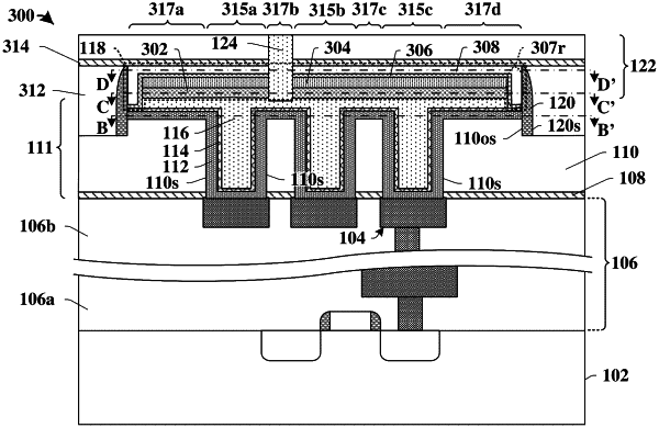
forming a capacitor stack over the first dielectric layer and within the plurality of openings, the capacitor stack comprising a capacitor dielectric layer between a lower electrode layer and an upper electrode layer, with the lower electrode layer having a recessed upper surface such that the recessed upper surface of the lower electrode layer is below an uppermost surface of the first dielectric layer;
etching the upper electrode layer of the capacitor stack to form an upper electrode, the upper electrode having an outer sidewall aligned over a location on the capacitor dielectric layer;
forming one or more capping layers to extend over the upper electrode layer and to extend along the outer sidewall of the upper electrode to contact the capacitor dielectric layer;
etching the one or more capping layers to define a capping structure over the upper electrode and to cutoff the lower electrode layer to form a lower electrode having an outer sidewall aligned with an outer sidewall of the capping structure; and
forming a spacer along the outer sidewall of the capping structure and along the outer sidewall of the lower electrode, the spacer including a lower surface that rests on an upper surface of the first dielectric layer;
wherein the spacer extends along the outer sidewall of the lower electrode, and the upper surface of the first dielectric layer steps down at an outer edge of the lower electrode to under an outer edge of the spacer.
|