| CPC H01L 21/7682 (2013.01) [H01L 21/0259 (2013.01); H01L 21/76805 (2013.01); H01L 21/76843 (2013.01); H01L 21/76895 (2013.01); H01L 23/5329 (2013.01); H01L 23/535 (2013.01); H01L 29/0665 (2013.01); H01L 29/41733 (2013.01); H01L 29/42392 (2013.01); H01L 29/66742 (2013.01); H01L 29/78618 (2013.01); H01L 29/78696 (2013.01)] | 20 Claims |

|
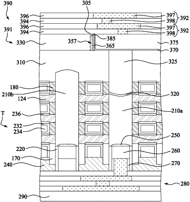
1. A method, comprising:
forming a transistor over a substrate;
forming a front-side interconnection structure over the transistor;
after forming the front-side interconnection structure, removing the substrate;
after removing the substrate, forming a backside via to be electrically connected to the transistor;
depositing a dielectric layer to cover the backside via;
forming an opening in the dielectric layer to expose the backside via;
forming a spacer structure on a sidewall of the opening;
after forming a spacer structure, forming a conductive feature in the opening to be electrically connected to the backside via; and
after forming the conductive feature, forming an air gap in the spacer structure.
|